
For applications requiring high-bandwidth camera interfaces, LogicTronix provides 8-lane MIPI-based FPGA designs built on Ultrascale+ and Versal architectures. These solutions support multi-camera configurations and high data rate transmission, making them suitable for advanced vision systems, autonomous platforms, and industrial imaging. Customers looking for scalable 4+ lane MIPI solutions can benefit from our optimized designs that balance performance, power, and flexibility.
For interfacing image sensors exceeding 40 megapixels or more than 4K resolution, significantly higher data throughput is required, which necessitates the use of an 8-lane MIPI pipeline. Such high-bandwidth designs typically demand support for 16-bit or higher data formats to preserve image quality and dynamic range.
In addition, achieving efficient processing at these data rates requires a pixels-per-clock (PPC) architecture greater than 4, ensuring the pipeline can handle the increased data volume without bottlenecks.
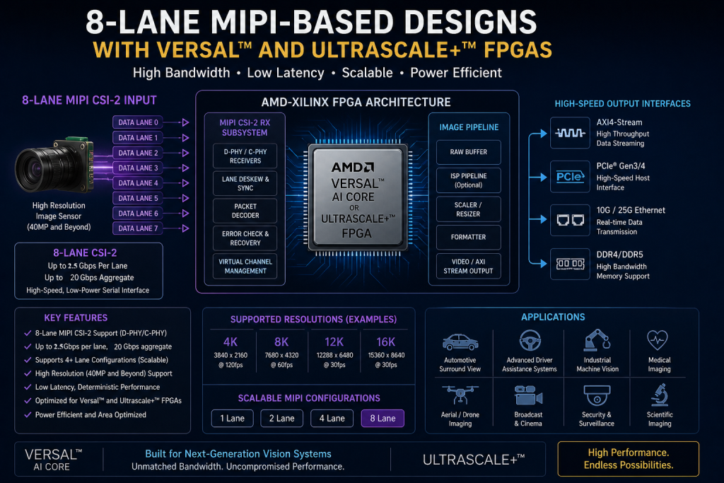
Figure – 8 Lane MIPI based design for high resolution sensors with Ultrascale+ or Versal
High-Bandwidth Image Acquisition Through 8-Lane MIPI CSI-2 with Ultrascale+ and Versal FPGA
At the input side, the architecture supports an 8-lane MIPI CSI-2 interface for connecting high-resolution image sensors.
The design shown supports up to:
- 2.5 Gbps to 3.2 Gb/s per MIPI lane
- 20 Gbps+ to 25.6 Gb/s aggregate bandwidth
- 4-lane and 8-lane scalable configurations
- High-resolution sensors rated at 40 MP and beyond
- Low-power, high-speed serial image transport
Each of the eight MIPI data lanes is independently received and routed into the FPGA’s MIPI CSI-2 receiver subsystem.
This makes the architecture suitable for demanding cameras where conventional lower-lane-count interfaces may not provide sufficient bandwidth.
FPGA-Based MIPI CSI-2 Receiver Subsystem
At the heart of the design is an AMD-Xilinx FPGA architecture, using either a Versal AI Core device or an UltraScale+ FPGA. The MIPI CSI-2 receiver subsystem is responsible for converting the incoming high-speed camera data into a form that can be processed by the FPGA fabric.
The architecture includes several functional blocks:
D-PHY / C-PHY Receivers
The physical-layer receivers provide the interface between the camera sensor and the FPGA.
Depending on the implementation and supported device capabilities, D-PHY or C-PHY technology can be used to receive high-speed MIPI traffic.
Lane Deskew and Synchronization
With multiple high-speed lanes operating in parallel, maintaining alignment between lanes is essential.
Lane deskew and synchronization compensate for timing differences between incoming lanes and ensure that image data can be reconstructed correctly.
Packet Decoder
CSI-2 data is transmitted using packets. The packet decoder interprets these packets and passes the relevant image information into the processing pipeline.
Error Checking and Recovery
The receiver architecture incorporates error checking and recovery mechanisms to improve robustness when handling high-speed serial data.
Virtual Channel Management
CSI-2 virtual channels allow multiple logical streams to share a physical interface. Virtual-channel management therefore provides additional flexibility for systems receiving multiple image or data streams.
From Raw Camera Data to Processed Images
Once the CSI-2 data has been received and decoded, it enters the FPGA’s image pipeline.
The architecture shown includes several processing stages.
Raw Buffer
Incoming image data can first be stored in a raw buffer, providing a controlled interface between the receiver and downstream processing stages.
Optional ISP Pipeline
An Image Signal Processor (ISP) can be incorporated when applications require operations such as image correction, enhancement, or sensor-specific processing.
Because the ISP is shown as optional, system designers can tailor the implementation according to their application and available FPGA resources.
Scaler and Resizer
The scaler/resizer enables image streams to be converted into different resolutions.
This can be particularly useful when a system needs to generate multiple output resolutions from a single high-resolution sensor.
Formatter
Image formatting prepares the processed data for downstream interfaces, accelerators, displays, storage, or other processing blocks.
Video / AXI Stream Output
The resulting image stream can be delivered through video or AXI-Stream interfaces, allowing the FPGA pipeline to connect efficiently with other hardware components.
Supporting Multiple Output Interfaces
High-speed image acquisition is only part of the challenge. Once the image has been captured and processed, the system needs to transfer the resulting data to other components.
The architecture provides several output options.
AXI4-Stream
AXI4-Stream provides a high-throughput internal or external streaming interface suitable for moving image data between FPGA processing blocks and other system components.
This is particularly useful for deeply pipelined FPGA architectures where data needs to move continuously between processing stages.
PCIe Gen3/Gen4
The design also supports PCIe Gen3/Gen4 connectivity for high-speed communication with a host processor or computing platform.
This allows processed image data to be transferred from the FPGA to a host system for additional analysis, AI inference, visualization, or storage.
10G / 25G Ethernet
For networked vision applications, 10GbE and 25GbE interfaces provide a path for real-time image-data transmission.
This can be valuable in distributed machine-vision systems where cameras and processing units are physically separated or where processed data must be shared across a high-speed network.
DDR4 / DDR5 Memory
High-bandwidth DDR4/DDR5 memory support provides external storage for frame buffers, intermediate image data, and other processing requirements.
Memory bandwidth becomes particularly important when working with very high-resolution frames or when multiple processing stages require access to image buffers.
Scalable MIPI Configurations
A major feature of the architecture is scalability.
The design illustrates support for:
1-lane → 2-lane → 4-lane → 8-lane MIPI configurations
This allows the same general architecture to be adapted to different camera sensors and bandwidth requirements.
For applications that do not require maximum bandwidth, a smaller lane configuration can reduce implementation complexity. For demanding high-resolution sensors, the full 8-lane configuration can provide substantially greater aggregate throughput.
Supporting High-Resolution Imaging
The architecture illustrates example processing targets ranging from 4K to 16K resolution.
| Resolution | Example Format | Example Frame Rate |
|---|---|---|
| 4K | 3840 × 2160 | Up to 120 fps |
| 8K | 7680 × 4320 | Up to 60 fps |
| 12K | 12288 × 6480 | Up to 30 fps |
| 16K | 15360 × 8640 | Up to 30 fps |
These figures represent example supported resolutions shown in the architecture rather than a universal performance guarantee for every FPGA or system implementation. Actual throughput depends on the selected FPGA, sensor, pixel format, processing pipeline, memory architecture, and implementation.
The ability to accommodate such high-resolution streams demonstrates the intended focus of the design: high-bandwidth, deterministic image processing at the edge.
Designed for Low-Latency Processing
For real-time vision applications, bandwidth alone is not enough. Latency is also critical.
The FPGA-based architecture allows image-processing functions to be implemented as hardware pipelines. Instead of relying entirely on sequential software processing, data can flow continuously through dedicated hardware stages.
This approach can provide:
- Predictable processing behavior
- Low and deterministic latency
- High data throughput
- Parallel image processing
- Efficient movement of streaming data
- Reduced dependence on a general-purpose CPU
These characteristics are particularly relevant to systems in which image information must be processed immediately after capture.
Why UltraScale+ and Versal FPGAs?
- High bandwidth — Multiple MIPI lanes provide a large aggregate data path from the image sensor.
- Low latency — Streaming hardware pipelines allow image data to move through processing stages without requiring large software-driven processing loops.
- Scalability — The architecture can be configured for different MIPI lane counts and processing requirements.
- Power efficiency — Dedicated hardware processing can perform highly parallel operations efficiently, which is important for embedded vision systems.