
LogicTronix HSB Enablement Services for AMD-Xilinx FPGA or Versal Adaptive SoCs
LogicTronix provides comprehensive Holoscan Sensor Bridge (HSB) enablement for AMD-Xilinx FPGA platforms (UltraScale+, MPSoC, and Versal), enabling seamless integration with NVIDIA Holoscan ecosystems for real-time sensor fusion and AI-driven applications.
As a critical pipeline for next-generation vision systems, HSB ensures efficient data flow between sensors and compute units. In addition, LogicTronix enhances FPGA pipelines across Lattice, Microchip, and Altera platforms, delivering optimized performance and flexibility for diverse edge AI and embedded vision deployments.
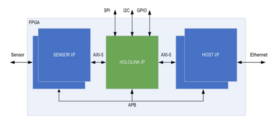
Figure – Holoscan Sensor Bridge IP Pipeline in FPGA [Source – NVIDIA]
Holoscan Sensor Bridge on AMD Xilinx FPGAs: High-Speed Sensor-to-AI Data Transfer
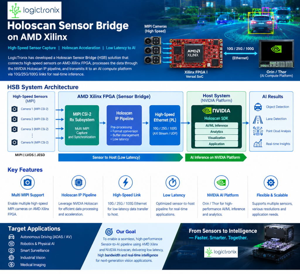
The article will distinguish between sensor acquisition and preprocessing on AMD-Xilinx FPGAs or Versal Adpative SoC and AI/ML inference on NVIDIA platforms, with a focus on high-throughput links such as 10G, 25G, and 100G Ethernet. It highlights the FPGA engineering capabilities in high-speed sensor interfacing, NVIDIA Holoscan integration, and low-latency data transfer to AI compute platforms such as NVIDIA Jetson AGX Orin and NVIDIA Jetson AGX Thor.
What is Holoscan Sensor Bridge?
The Holoscan Sensor Bridge (HSB) is an architectural approach for connecting high-speed sensors to NVIDIA Holoscan-based AI processing systems. It enables sensor data to be acquired and prepared on an AMD-Xilinx FPGA (UltraScale+, MPSoC, and Versal) before being transmitted to an NVIDIA host system for downstream AI/ML processing.
The objective is to build a high-throughput, low-latency path from the sensor to the AI compute platform while minimizing unnecessary data movement and processing overhead.
Key Capabilities
1. Multiple MIPI/LVDS/SLVS-EC or JESD sensor integration
LogicTronix works on enabling multiple high-speed MIPI camera interfaces on AMD-Xilinx FPGA platforms. FPGA-based capture pipelines can be designed to support parallel sensor streams, synchronization, and application-specific preprocessing.
Potential capabilities include:
- Multi-camera MIPI CSI-2/LVDS/SLVS-EC or JESD reception.
- High-throughput pixel and sensor data handling.
- Sensor synchronization and stream alignment.
- FPGA-based format conversion and preprocessing.
2. FPGA-based sensor data processing and Hololink IP Integration
The AMD-Xilinx FPGA serves as a programmable data-processing layer between the sensors and the AI compute platform.
Depending on application requirements, the FPGA pipeline can perform:
- Data reformatting and packing.
- Image preprocessing.
- Stream synchronization.
- Metadata handling.
- Buffer management and data-path optimization.
- Integrating the sensor data pipeline to Hololink IP and interface from NVIDIA
This approach allows sensor data to be prepared for efficient transmission to the host.
3. High-speed 10G, 25G/40G, and 100G connectivity
To support demanding sensor workloads, the architecture targets high-speed Ethernet connectivity between the FPGA and the NVIDIA host platform.
| Link | Potential role |
|---|---|
| 10GbE | Sensor streaming and moderate-bandwidth applications |
| 25/40GbE | High-throughput multi-sensor data transfer |
| 100GbE | Large-scale sensor fusion and high-bandwidth perception systems |
Ethernet connectivity leverages RDMA over Converged Ethernet (RoCEv2) to enable highly optimized, low-latency data transfers while minimizing traditional networking overhead.
Actual throughput depends on the selected Ethernet architecture, protocol overhead, sensor formats, and hardware implementation.
4. Low-latency sensor-to-host transfer
The HSB pipeline is targeted at minimizing the time between sensor data acquisition and the availability of data on the NVIDIA AI compute platform.
The design focus includes:
- Efficient FPGA-to-host data movement.
- Reduced unnecessary copies and transformations.
- Stream-oriented processing.
- High-bandwidth transport.
- Coordinated sensor data and metadata transfer.
The goal is to provide the NVIDIA AI platform with sensor data as efficiently as possible, enabling low-latency AI/ML applications.
Target Applications
Autonomous Driving and ADAS
Multi-camera acquisition, perception pipelines, and sensor fusion using NVIDIA AI compute platforms.

Robotics and Physical AI
High-speed visual sensing and real-time AI processing for robotic systems.

Industrial Vision
High-bandwidth camera streams for inspection, monitoring, and intelligent automation.

Advanced Imaging Systems
Low-latency sensor acquisition and high-speed transfer for demanding imaging applications.

LogicTronix Engineering Expertise
LogicTronix brings FPGA design and embedded systems expertise to the development of high-performance sensor-processing solutions.
Our areas of work on HSB Pipeline enablement include:
- AMD-Xilinx FPGA and Versal platform development.
- Multi-MIPI camera interface integration.
- FPGA-based image and sensor data processing.
- High-speed Ethernet data paths.
- Custom hardware acceleration and streaming pipelines.
- Integration of FPGA sensor systems with NVIDIA AI platforms via Holoscan Sensor Bridge Pipeline.
- Performing AI inference , optimization and fusion for real-world applications as ADAS, AMR , Physical AI etc.
Our goal is to help organizations build scalable, high-performance sensor-to-AI architectures for next-generation perception and intelligent computing applications.
Conclusion
The combination of AMD-Xilinx FPGA-based sensor processing and NVIDIA Holoscan-enabled AI computing creates an opportunity to design flexible, high-bandwidth sensor-to-host systems.
With support for multiple MIPI sensors and targeted 10G, 25G/40G, and 100G connectivity, LogicTronix is exploring architectures that address the demands of modern autonomous systems, robotics, and real-time AI applications.
From high-speed sensor capture to AI-powered intelligence, LogicTronix helps bridge the gap between physical-world data and next-generation computing platforms.